- 您现在的位置:买卖IC网 > Sheet目录487 > NTD4906NT4G (ON Semiconductor)MOSFET N-CH 30V 10.3A SGL DPAK
�� �
�
�NTD4906N�
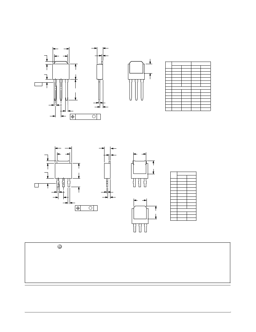
�PACKAGE� DIMENSIONS�
�IPAK� (STRAIGHT� LEAD� DPAK)�
�CASE� 369D�
�ISSUE� C�
�V�
�B�
�R�
�C�
�E�
�NOTES:�
�1.� DIMENSIONING� AND� TOLERANCING� PER�
�ANSI� Y14.5M,� 1982.�
�2.� CONTROLLING� DIMENSION:� INCH.�
�S�
�?� T� ?�
�SEATING�
�PLANE�
�1�
�4�
�2�
�3�
�A�
�K�
�Z�
�DIM�
�A�
�B�
�C�
�D�
�E�
�F�
�G�
�H�
�J�
�K�
�INCHES�
�MIN� MAX�
�0.235� 0.245�
�0.250� 0.265�
�0.086� 0.094�
�0.027� 0.035�
�0.018� 0.023�
�0.037� 0.045�
�0.090� BSC�
�0.034� 0.040�
�0.018� 0.023�
�0.350� 0.380�
�MILLIMETERS�
�MIN� MAX�
�5.97� 6.35�
�6.35� 6.73�
�2.19� 2.38�
�0.69� 0.88�
�0.46� 0.58�
�0.94� 1.14�
�2.29� BSC�
�0.87� 1.01�
�0.46� 0.58�
�8.89� 9.65�
�F�
�G�
�J�
�D� 3� PL�
�0.13� (0.005)�
�M�
�T�
�H�
�STYLE� 2:�
�PIN� 1.� GATE�
�2.� DRAIN�
�3.� SOURCE�
�4.� DRAIN�
�R�
�S�
�V�
�Z�
�0.180� 0.215�
�0.025� 0.040�
�0.035� 0.050�
�0.155� ???�
�4.45� 5.45�
�0.63� 1.01�
�0.89� 1.27�
�3.93� ???�
�3.5� MM� IPAK,� STRAIGHT� LEAD�
�CASE� 369AD�
�ISSUE� B�
�L2�
�L1�
�E�
�E3�
�D�
�A�
�A1�
�E2�
�D2�
�NOTES:�
�1..� DIMENSIONING� AND� TOLERANCING� PER�
�ASME� Y14.5M,� 1994.�
�2..� CONTROLLING� DIMENSION:� MILLIMETERS.�
�3.� DIMENSION� b� APPLIES� TO� PLATED� TERMINAL�
�AND� IS� MEASURED� BETWEEN� 0.15� AND�
�0.30mm� FROM� TERMINAL� TIP.�
�4.� DIMENSIONS� D� AND� E� DO� NOT� INCLUDE�
�MOLD GATE OR MOL� D� FLASH.�
�MILLIMETERS�
�T�
�L�
�DIM�
�A�
�A1�
�A2�
�MIN� MAX�
�2.19� 2.38�
�0.46� 0.60�
�0.87� 1.10�
�SEATING�
�PLANE�
�b1�
�2X� e�
�3X�
�b�
�0.13�
�M�
�T�
�A1�
�A2�
�E2�
�D2�
�b�
�b1�
�D�
�D2�
�E�
�E2�
�E3�
�e�
�L�
�L1�
�L2�
�0.69� 0.89�
�0.77� 1.10�
�5.97� 6.22�
�4.80� ???�
�6.35� 6.73�
�4.57� 5.45�
�4.45� 5.46�
�2.28� BSC�
�3.40� 3.60�
�???� 2.10�
�0.89� 1.27�
�OPTIONAL�
�CONSTRUCTION�
�ON� Semiconductor� and� are� registered� trademarks� of� Semiconductor� Components� Industries,� LLC� (SCILLC).� SCILLC� owns� the� rights� to� a� number� of� patents,� trademarks,�
�copyrights,� trade� secrets,� and� other� intellectual� property.� A� listing� of� SCILLC’s� product/patent� coverage� may� be� accessed� at� www.onsemi.com/site/pdf/Patent� ?� Marking.pdf.� SCILLC�
�reserves� the� right� to� make� changes� without� further� notice� to� any� products� herein.� SCILLC� makes� no� warranty,� representation� or� guarantee� regarding� the� suitability� of� its� products� for� any�
�particular� purpose,� nor� does� SCILLC� assume� any� liability� arising� out� of� the� application� or� use� of� any� product� or� circuit,� and� specifically� disclaims� any� and� all� liability,� including� without�
�limitation� special,� consequential� or� incidental� damages.� “Typical”� parameters� which� may� be� provided� in� SCILLC� data� sheets� and/or� specifications� can� and� do� vary� in� different� applications�
�and� actual� performance� may� vary� over� time.� All� operating� parameters,� including� “Typicals”� must� be� validated� for� each� customer� application� by� customer’s� technical� experts.� SCILLC�
�does� not� convey� any� license� under� its� patent� rights� nor� the� rights� of� others.� SCILLC� products� are� not� designed,� intended,� or� authorized� for� use� as� components� in� systems� intended� for�
�surgical� implant� into� the� body,� or� other� applications� intended� to� support� or� sustain� life,� or� for� any� other� application� in� which� the� failure� of� the� SCILLC� product� could� create� a� situation� where�
�personal� injury� or� death� may� occur.� Should� Buyer� purchase� or� use� SCILLC� products� for� any� such� unintended� or� unauthorized� application,� Buyer� shall� indemnify� and� hold� SCILLC� and�
�its� officers,� employees,� subsidiaries,� affiliates,� and� distributors� harmless� against� all� claims,� costs,� damages,� and� expenses,� and� reasonable� attorney� fees� arising� out� of,� directly� or� indirectly,�
�any� claim� of� personal� injury� or� death� associated� with� such� unintended� or� unauthorized� use,� even� if� such� claim� alleges� that� SCILLC� was� negligent� regarding� the� design� or� manufacture�
�of� the� part.� SCILLC� is� an� Equal� Opportunity/Affirmative� Action� Employer.� This� literature� is� subject� to� all� applicable� copyright� laws� and� is� not� for� resale� in� any� manner.�
�PUBLICATION� ORDERING� INFORMATION�
�LITERATURE� FULFILLMENT� :�
�Literature� Distribution� Center� for� ON� Semiconductor�
�P.O.� Box� 5163,� Denver,� Colorado� 80217� USA�
�Phone� :� 303� ?� 675� ?� 2175� or� 800� ?� 344� ?� 3860� Toll� Free� USA/Canada�
�Fax� :� 303� ?� 675� ?� 2176� or� 800� ?� 344� ?� 3867� Toll� Free� USA/Canada�
�Email� :� orderlit@onsemi.com�
�N.� American� Technical� Support� :� 800� ?� 282� ?� 9855� Toll� Free�
�USA/Canada�
�Europe,� Middle� East� and� Africa� Technical� Support:�
�Phone:� 421� 33� 790� 2910�
�Japan� Customer� Focus� Center�
�Phone:� 81� ?� 3� ?� 5817� ?� 1050�
�http://onsemi.com�
�8�
�ON� Semiconductor� Website� :� www.onsemi.com�
�Order� Literature� :� http://www.onsemi.com/orderlit�
�For� additional� information,� please� contact� your� local�
�Sales� Representative�
�NTD4906N/D�
�发布紧急采购,3分钟左右您将得到回复。
相关PDF资料
NTD4909NT4G
MOSFET N-CH 30V 8.8A SGL DPAK
NTD4910NT4G
MOSFET N-CH 30V 37A DPAK
NTD4913NT4G
MOSFET N-CH 30V 32A DPAK
NTD4959NT4G
MOSFET N-CH 30V 9A TP-FA
NTD4960NT4G
MOSFET N-CH 30V 11.1A DPAK
NTD4965NT4G
MOSFET N-CH 30V 68A DPAK
NTD4970N-35G
MOSFET N-CH 30V 38A IPAK
NTD50N03RT4G
MOSFET N-CH 25V 7.8A DPAK
相关代理商/技术参数
NTD4909N
制造商:ONSEMI 制造商全称:ON Semiconductor 功能描述:Power MOSFET 30 V, 41 A, Single N−Channel, DPAK/IPAK
NTD4909N-1G
功能描述:MOSFET NFET DPAK 30V 41A 8.0 mOhm RoHS:否 制造商:STMicroelectronics 晶体管极性:N-Channel 汲极/源极击穿电压:650 V 闸/源击穿电压:25 V 漏极连续电流:130 A 电阻汲极/源极 RDS(导通):0.014 Ohms 配置:Single 最大工作温度: 安装风格:Through Hole 封装 / 箱体:Max247 封装:Tube
NTD4909N-35G
功能描述:MOSFET NFET DPAK 30V 41A 8.0 mOhm RoHS:否 制造商:STMicroelectronics 晶体管极性:N-Channel 汲极/源极击穿电压:650 V 闸/源击穿电压:25 V 漏极连续电流:130 A 电阻汲极/源极 RDS(导通):0.014 Ohms 配置:Single 最大工作温度: 安装风格:Through Hole 封装 / 箱体:Max247 封装:Tube
NTD4909NA-1G
功能描述:MOSFET NFET DPAK 30V 41A 8 mOhm RoHS:否 制造商:STMicroelectronics 晶体管极性:N-Channel 汲极/源极击穿电压:650 V 闸/源击穿电压:25 V 漏极连续电流:130 A 电阻汲极/源极 RDS(导通):0.014 Ohms 配置:Single 最大工作温度: 安装风格:Through Hole 封装 / 箱体:Max247 封装:Tube
NTD4909NA-35G
功能描述:MOSFET NFET DPAK 30V 41A 8 mOhm RoHS:否 制造商:STMicroelectronics 晶体管极性:N-Channel 汲极/源极击穿电压:650 V 闸/源击穿电压:25 V 漏极连续电流:130 A 电阻汲极/源极 RDS(导通):0.014 Ohms 配置:Single 最大工作温度: 安装风格:Through Hole 封装 / 箱体:Max247 封装:Tube
NTD4909NAT4G
功能描述:MOSFET NFET DPAK 30V 41A 8.0 mOhm RoHS:否 制造商:STMicroelectronics 晶体管极性:N-Channel 汲极/源极击穿电压:650 V 闸/源击穿电压:25 V 漏极连续电流:130 A 电阻汲极/源极 RDS(导通):0.014 Ohms 配置:Single 最大工作温度: 安装风格:Through Hole 封装 / 箱体:Max247 封装:Tube
NTD4909NAT4H
制造商:Rochester Electronics LLC 功能描述: 制造商:ON Semiconductor 功能描述:
NTD4909NT4G
功能描述:MOSFET NFET DPAK 30V 41A 8.0 mOhm RoHS:否 制造商:STMicroelectronics 晶体管极性:N-Channel 汲极/源极击穿电压:650 V 闸/源击穿电压:25 V 漏极连续电流:130 A 电阻汲极/源极 RDS(导通):0.014 Ohms 配置:Single 最大工作温度: 安装风格:Through Hole 封装 / 箱体:Max247 封装:Tube